Everything from the designing of patterns for printed circuit boards to the production of printed circuit boards is carried out on an integrated basis under one roof.

Renowned as a castle town on the Shonai Plains, Tsuruoka City, Yamagata Prefecture, is home to many companies with ties to the automotive and communications sectors. OKI Circuit Technology’s head office and plant are located in an industrial park not far from JR East Tsuruoka Station and have been manufacturing printed circuit boards since 1980.

Printed circuit boards are electronic parts made by forming circuits with conductive metal foil on boards as the base. Electronic circuits are formed by soldering electronic parts—integrated circuit chips, resistors, condensers, and transformers—onto printed circuit boards. Solder is sometimes coated to achieve a better flow onto circuit parts while gold plating is sometimes applied for improved electric conductivity.

Before printed circuit boards were introduced to Japan in the 1930s, electronic circuits were formed by connecting individual parts to one another with electric wire. By using printed circuit boards, complex circuits can be more easily manufactured and completed circuits are miniaturized. When first introduced, they consisted merely of a single-layer substrate formed by applying a copper circuit pattern to the surface of the base. Later, both sides came to be used. This was followed up by the insertion of insulating material in a way that allowed multiple layers of fine circuit patterns to be stacked atop one another. The printed circuit boards manufactured by OKI Circuit Technology currently consist of up to 50 of these layers with a single wire miniaturized to 50 micrometers in width. The base consists of rigid boards, as well as boards made from flexible, supple materials.

Once wiring is miniaturized to this extent, an extensive accumulation of expertise is required in terms of design and production. For example, parts through which high-frequency signals pass require that the signal transmission speed be controlled by using materials with a low dielectric constant. This company endeavors, as a full-time manufacturer of printed circuit boards, to accumulate such knowledge by carrying out everything from the design of patterns to the production of printed circuit boards on an integrated basis under one roof.

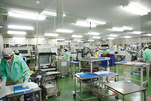
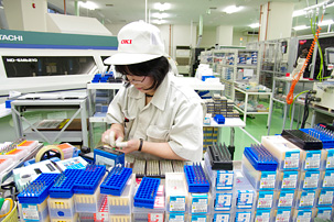
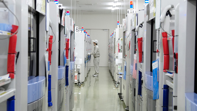
While up to 200 different types of substrates are manufactured each day, approximately 30 on average of any given type are produced. The plant is a picture of extreme contrast between the large number of types and the small volume of each type that are manufactured. For this reason, printed circuit boards for space applications are inserted into gaps for the production of printed circuit boards for industrial purposes and are manufactured according to special procedures for space. Reliability is heavily emphasized for printed circuit boards for space applications.

The company has obtained certification for printed circuit boards from JAXA for up to 10 layers. In the future, the company expects to have the scope of certification expanded.

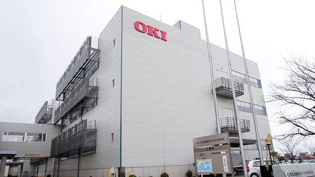
Situated in Tsuruoka City, Yamagata Prefecture, the head office and plant of OKI Circuit Technology has produced printed circuit boards since 1980, back when it was known as Tanaka Kikinzokup>

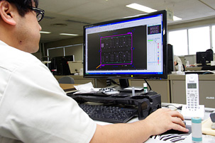
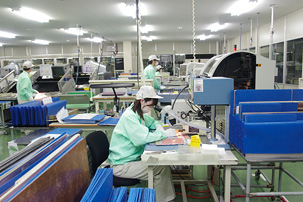
Patterns for printed circuit boards are developed and designed with CAD (computer-aided design) software according to client needs.

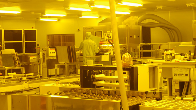
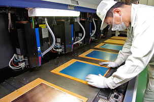
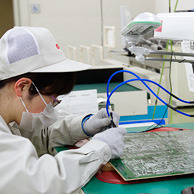
Substrate patterns are subject to a printing process that occurs in a class 10,000 clean room, where light of a non-photosensitive wavelength region is used.

OKI左抜け

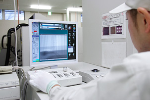
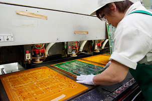
Substrates for which parts other than a printed pattern are removed through etching are inspected (left) and, if required, fixed (right).)

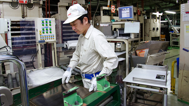
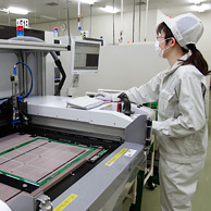
Substrates on which patterns have been formed are layered in a press machine. The company manufactures high-performance printed circuit boards with up to 44 layers.

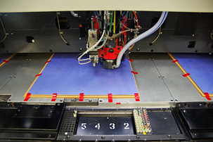
In the perforation process, lead insertion holes or mounting holes for electronic parts are created with a drilling processing machine.

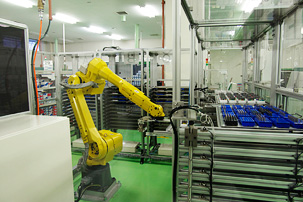
Drills for printed circuit boards whose production quantity is relatively high are supplied by a robot (left).
In contrast, this process relies on the involvement of human beings for printed circuit boards characterized by the production of many kinds in small quantities (right).

An X-ray inspection device is used to determine whether holes have been drilled in the correct positions on each substrate and for other checks.(left)
Router processing is carried out to fabricate the outline, openings, and other elements of each substrate.(right)

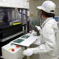
Wiring testers are used to inspect the continuity and open circuitry of manufactured printed circuit boards. The company employs an array of 18 units.

Impedance testing is shown in these photographs. Two types of testing machines (left and middle) and manual testing (right) are properly employed according to the volume of production.

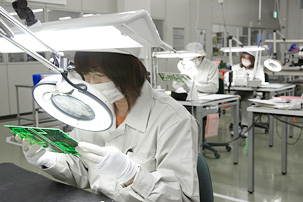
The external appearance of each printed circuit is visually inspected. Such a strict system of inspections underpins the high level of quality of the printed circuit boards manufactured by this company.(Left).
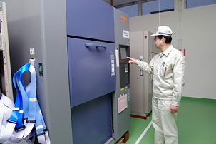
Thermal shock testing equipment is used to carry out approximately 1,000 repeated cycles of thermal shock testing on printed circuit boards for space applications.(Right)

OKI CIRCUIT TECHNOLOGY Co., Ltd.

Location of head office Tsuruoka City, Yamagata Prefecture
Year of establishment 2012
Main manufacturing sites Head office and plant (Tsuruoka City, Yamagata Prefecture)
Main products High-performance printed circuit boards
Main space equipment that the company has helped produce to date Printed circuit boards mounted on satellites
Company website http://www.oki-otc.jp/

INTERVIEW

インタビュー

Printed circuit boards for space applicationsare subject to testing that is ten times as strictas testing for conventional circuit boards.

OKI CIRCUIT TECHNOLOGY
Executive officer,general manager of production department
kazuyuki Saito

--It seems that you are a very new company.

That is correct. We are a manufacturer of printed circuit boards for use in precision electronic equipment but were a division of Tanaka Kikinzoku Kogyo until September 30, 2012. Beginning on October 1, 2012, we were reborn as a new company in the OKI Group. OKI owns an 80 percent stake in our company while Tanaka Kikinzoku Kogyo retains a 20 percent stake. We can trace our roots to Pilot Chemical, a company that was established in 1970 through a merger between Tanaka Kikinzoku Kogyo and Pilot Ink. We later became a division of Tanaka Kikinzoku Kogyo in 1980.

--Around when did you start producing printed circuit boards for space applications?

Tanaka Kikinzoku Kogyo had previously entered the field of space. As an example, a noble metal-based brazing filler used to assemble and connect rocket engines is a product manufactured by Tanaka Kikinzoku Kogyo. The following describes what prompted us to enter the field of space through our printed circuit board business. In assuming that products for manufacture in the future would be subject to greater demand for high levels of reliability, we obtained certification as granted by what was then known as NASDA (National Space Development Agency of Japan) in 2001.

--What was the impetus that led you to obtain this certification?

We sought to obtain certification in order to direct the attention of our clients to the quality of our products. Our products consist almost entirely of high-performance printed circuit boards for industrial applications. We do not produce printed circuit boards for consumer equipment like household electrical appliances. We supply a wide variety of products in small quantities for use in the social infrastructure, communication equipment, measuring equipment, and semiconductor testers. In giving an example that most anyone can relate to, our printed circuit boards are also used in the signs that display train times and destinations in the train stations.

When it comes to printed circuit boards for industrial applications, there is nothing more important than high levels of quality and reliability. We have obtained ISO 9001 and ISO 14001 certification for quality control and environmental management from the International Organization for Standardization. Yet, as these standards came to be adopted by more and more enterprises, we found it increasingly difficult to differentiate ourselves on this basis alone. In this connection, we wondered whether we could obtain certification under the category of space in order to direct the attention of others to the high levels of quality and reliability of our products. Of course, we were not simply aiming to reap the advertising benefits of being able to declare that we obtained certification in the field of space. We received our first order for printed circuit boards for space applications in 2003. From that point forth, we gradually found our products being used to a greater extent even in the field of space.

Our competitive advantage lies in our integrated approach to carrying out everything from the design to the production of printed circuit boards. Since everything is carried out on an integrated basis, we are not only able to realize a high level of quality, but we are also able to complete difficult jobs for quick delivery. For this reason, the belief on the part of our clients that they receive value that is fully commensurate with the price we charge has become essential for our growth. Given these factors, we turned our attention to the new field of space.

--Have printed circuit boards made by your company been installed in space equipment before?

We receive orders for printed circuit boards from manufacturers of electronic equipment mounted on satellites and make deliveries accordingly. Circuit schematics and specifications are shown to us when orders are received but we are not told with what satellites our products will be used. Thus, we are generally not aware of which satellites our printed circuit boards are used.

--What are the differences between printed circuit boards for space applications and printed circuit boards for other industrial uses?

Printed circuit boards for space applications are subject to very strict demands for a high level of reliability. To illustrate, look at usage temperatures. Printed circuit boards are subject to thermal shock testing whereby they are exposed repeatedly to a cycle of high and low temperatures ranging from 125 degrees Celsius to minus 30 degrees Celsius. Printed circuit boards for general industrial purposes typically undergo testing that consists of 100 to 300 cycles (though this will depend on the client). In contrast, printed circuit boards for space applications are required to undergo 1,000 cycles without breaking. Even with printed circuit boards for general industrial purposes, we have met rather strict conditions for supplying such products for use in extreme environments as substrates for electronic devices in electric power stations. The basic technologies that we cultivated in meeting these conditions have helped us to develop products for space applications. At the same time, we have also been required to implement traceability according to highly rigid standards. We are obliged to retain a manufacturing history for products for a period of seven years after the product has been manufactured.

--What is your outlook or vision for the future of the field of space?

Our sales for the field of space amounts to no more than 4 percent of our total sales. We would like to increase this figure to at least 10 percent in three years by expanding the volume of orders we receive.

--Could you share with us anything that you would like to see from JAXA towards the fulfillment of your vision for the future?

JAXA’s certification is not something for which efforts come to an end once granted. Rather, it is something that must be obtained again if conditions change. We would like to have a plan for updating certification to make it easier after a change in conditions. Occasionally, a materials manufacturer withdraws from JAXA’s list of certified materials, which necessitates a switch from a material that we had been using to another alternative material. In such a case, we are required to re-obtain certification. Since this imposes significant time and labor demands for each change, we would appreciate it if change procedures of this type could be simplified for our benefit.

RELATED

関連記事