Optical semiconductor detector
development starts with materials
Hamamatsu TV, the predecessor of Hamamatsu Photonics, was established in Hamamatsu, Shizuoka Prefecture in 1953 by three people including Heihachiro Horiuchi, a disciple of Professor Kenjiro Takayanagi at the Hamamatsu College of Engineering (now the Faculty of Engineering at Shizuoka University), the “father of Japanese television” who built the world’s first cathode ray tube (CRT) television. Since then, the company has established a name for itself through research and development of optical-related products including phototubes, as well as photomultiplier tubes (PMTs), video camera tubes, photodiodes, photonic integrated circuits and image-sensing semiconductors and other products.
Hamamatsu Photonics has recently expanded into the medical and bio fields by using optics and X-ray technology to make inspection and testing equipment. In 1996, the company delivered 11,200 20-inch PMTs for Super-Kamiokande neutrino detectors. It is known that Professor Emeritus Masatoshi Koshiba of the University of Tokyo won the Nobel Prize in Physics in 2002 for his research using this equipment.
In the space sector, Hamamatsu Photonics’ rocket tracking system that utilizes high-speed television cameras, X-ray charge-coupled devices (CCDs), visible light and near-infrared semiconductor sensors and other products are widely used for the Earth observation satellites, astronomical satellites, the International Space Station (ISS) and elsewhere.
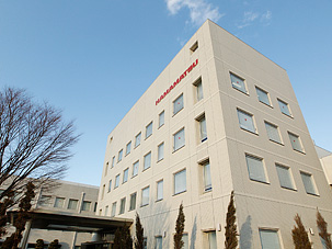
The company’s headquarters in Hamamatsu is the core of its image-sensing semiconductor business. Most of its space sensors are also made here.
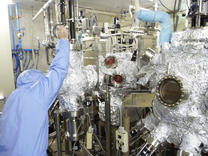
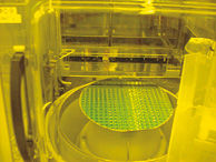
Molecular beam epitaxy (MBE) equipment used to grow semiconductor crystals. Hamamatsu Photonics gets involved at the materials development phase in order to develop new optical semiconductor detectors.
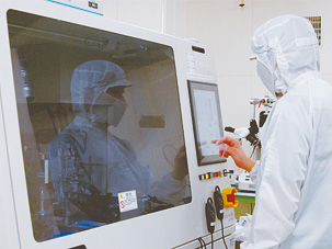
This is a metal organic chemical vapor deposition (MOCVD) device. Along with the MBE device, this is used to grow crystals.
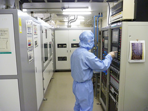
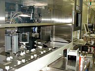
This plasma chemical vapor deposition (PCVD) machine forms thin film to produce various insulating and protective film for semiconductor devices.
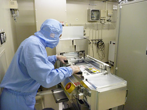
Photolithography is used to transcribe optical semiconductor device patterns.
Ions are injected into wafers to change semiconductor properties.
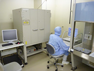
After optical semiconductor device wafers are completed, the device’s optical properties are measured and assessed.
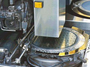
After wafers are made, they move on to the assembly process, where they are cut into chips by circular rotary blades.
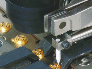
The die bonding process affixes each chip to a metal base.
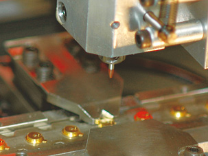
The wire bonding process connects the metal base and the chip with a gold wire.
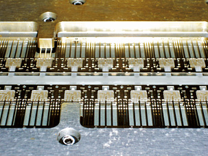
In addition to a metal package, an image-sensing semiconductor has various packages such as a ceramic package and a plastic package and more. This photo shows the process by which a chip is sealed with resin on a lead frame in a plastic package.
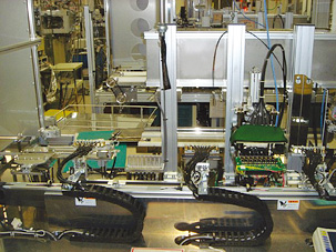
This machine inspects image sensing in completed plastic chip packages.
Flip chip bonding joins chips with a board in a chip size package production process that employs small and thin chips as needed.
HAMAMATSU PHOTONICS
INTERVIEW
インタビュー
We're always developing
new optical sensors used for space
HAMAMATSU PHOTONICS
Solid State Division, No.1, Solid State Production Director
Akimasa Tanaka
